
Report an Error
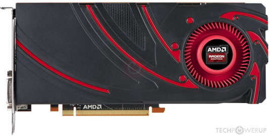

AMD Radeon R9 285
- Graphics Processor
- Tonga
- Cores
- 1792
- TMUs
- 112
- ROPs
- 32
- Memory Size
- 2 GB
- Memory Type
- GDDR5
- Bus Width
- 256 bit


GPU
Recommended Gaming Resolutions:
- 1366x768
- 1600x900
- 1920x1080
The Radeon R9 285 was a performance-segment graphics card by AMD, launched on September 2nd, 2014. Built on the 28 nm process, and based on the Tonga graphics processor, in its Tonga PRO variant, the card supports DirectX 12. This ensures that all modern games will run on Radeon R9 285. The Tonga graphics processor is a large chip with a die area of 366 mm² and 5.00 billion transistors. Unlike the fully unlocked Radeon R9 285X, which uses the same GPU but has all 2048 shaders enabled, AMD has disabled some shading units on the Radeon R9 285 to reach the product's target shader count. It features 1792 shading units, 112 texture mapping units, and 32 ROPs. AMD has paired 2,048 MB GDDR5 memory with the Radeon R9 285, which is connected using a 256-bit memory interface. The GPU is operating at a frequency of 918 MHz, memory is running at 1375 MHz (5.5 Gbps effective).
Being a dual-slot card, the AMD Radeon R9 285 draws power from 2x 6-pin power connectors, with power draw rated at 190 W maximum. Display outputs include: 2x DVI, 1x HDMI 1.4a, 1x DisplayPort 1.2. Radeon R9 285 is connected to the rest of the system using a PCI-Express 3.0 x16 interface. The card's dimensions are 221 mm x 109 mm x 36 mm, and it features a dual-slot cooling solution. Its price at launch was 249 US Dollars.
Being a dual-slot card, the AMD Radeon R9 285 draws power from 2x 6-pin power connectors, with power draw rated at 190 W maximum. Display outputs include: 2x DVI, 1x HDMI 1.4a, 1x DisplayPort 1.2. Radeon R9 285 is connected to the rest of the system using a PCI-Express 3.0 x16 interface. The card's dimensions are 221 mm x 109 mm x 36 mm, and it features a dual-slot cooling solution. Its price at launch was 249 US Dollars.
Graphics Processor
Graphics Card
- Release Date
- Sep 2nd, 2014
- Generation
-
Volcanic Islands
(R9 200)
- Predecessor
- Sea Islands
- Successor
- Pirate Islands
- Production
- End-of-life
- Launch Price
- 249 USD
- Bus Interface
- PCIe 3.0 x16
- Reviews
- 59 in our database
Relative Performance
Based on TPU review data: "Performance Summary" at 1920x1080, 4K for RTX 3080 and faster.
Clock Speeds
- GPU Clock
- 918 MHz
- Memory Clock
-
1375 MHz
5.5 Gbps effective
Memory
- Memory Size
- 2 GB
- Memory Type
- GDDR5
- Memory Bus
- 256 bit
- Bandwidth
- 176.0 GB/s
Render Config
- Shading Units
- 1792
- TMUs
- 112
- ROPs
- 32
- Compute Units
- 28
- L1 Cache
- 16 KB (per CU)
- L2 Cache
- 512 KB
Theoretical Performance
- Pixel Rate
- 29.38 GPixel/s
- Texture Rate
- 102.8 GTexel/s
- FP16
- 3.290 TFLOPS (1:1)
- FP32
- 3.290 TFLOPS
- FP64
- 205.6 GFLOPS (1:16)
Numeric Format Support
- Vector
-
INT4INT8INT16INT32FP16BF16FP32FP64
- Matrix
- Not Supported
Board Design
- Slot Width
- Dual-slot
- Length
- 221 mm
8.7 inches
- Height
- 109 mm
4.3 inches
- Width
- 36 mm
1.4 inches
- TDP
- 190 W
- Suggested PSU
- 450 W
- Outputs
- 2x DVI
1x HDMI 1.4a
1x DisplayPort 1.2
- Power Connectors
- 2x 6-pin
- Board Number
- C766
Graphics Features
- DirectX
- 12 (12_0)
- OpenGL
- 4.6
- OpenCL
- 2.0
- Vulkan
- 1.2.170
- Shader Model
- 6.5
Tonga GPU Notes
| Generation: Volcanic Islands Desktop Variant: Antigua Mobile Variant: Amethyst Shader ISA: GFX8 (gfx802) Graphics/Compute: 8.0.0 Display Controller Engine: 10.0.0 Unified Video Decoder: 5.0.0 Video Coding Engine: 3.0.0 Latest Drivers: Windows 7: 64-bit: AMD Software: Adrenalin Edition 22.6.1 Windows 8.1: 64-bit: Radeon Software: Crimson ReLive Edition 17.4.4 / 17.7.1 Windows 10: 64-bit: AMD Software: Adrenalin Edition 22.6.1 |
Retail boards based on this design (14)
| Name | GPU Clock | Memory Clock | Other Changes |
|---|---|---|---|
| 954 MHz | 1375 MHz | 269 mm/10.6 inches | |
| 945 MHz | 1375 MHz | 225 mm/8.9 inches | |
| 973 MHz | 1375 MHz | ||
| 938 MHz | 1375 MHz | 270 mm/10.6 inches | |
| 938 MHz | 1375 MHz | 210 mm/8.3 inches | |
| 973 MHz | 1375 MHz | 263 mm/10.4 inches | |
| 945 MHz | 1375 MHz | 207 mm/8.1 inches | |
| 918 MHz | 1375 MHz | 264 mm/10.4 inches | |
| 965 MHz | 1400 MHz | 264 mm/10.4 inches | |
| 918 MHz | 1375 MHz | 171 mm/6.7 inches, 1x DVI 1x HDMI 2x mini-DisplayPort | |
| 928 MHz | 1375 MHz | 171 mm/6.7 inches, 1x DVI 1x HDMI 2x mini-DisplayPort | |
| 945 MHz | 1375 MHz | 207 mm/8.1 inches | |
| 975 MHz | 1375 MHz | ||
| 918 MHz | 1375 MHz |


Oct 22nd, 2026 20:57 EDT
change timezone
Latest GPU Drivers

New Forum Posts
- Privacy Clubhouse (6)
- MooBench - Benchmark Automation Software (0)
- Ryzen 5 5600 + RX 7700 XT – Micro-Stuttering and Poor 1% Lows (7)
- What Speakers Are You You Using For Your Computer (270)
- Windows 11 General Discussion (7671)
- Can you guess Which game it is? (307)
- Big tech calling for AI slowdown (87)
- Any other old-timers here planning to play WoW Forever? (111)
- Free Games Thread (5361)
- I can't find a solution to the frame skipping and micro stuttering. (43)

Popular Reviews
- Cooler Master HAF II 500 Review
- AMD Ryzen AI Halo Review - Local-AI Powerhouse with 128 GB of Memory
- ASRock Z890 Taichi Aqua Review
- FSP MEGA PM 1200W Review
- Upcoming Hardware Launches 2026 (Updated Jul 2026)
- Pulsar Feinmann F01 Noctua Edition Review
- Corsair VANGUARD AIR 99 WIRELESS Keyboard Review
- LattePanda Mu Ultra Review
- AMD Ryzen 7 9800X3D Review - The Best Gaming Processor
- Gears of War: E-Day Performance Benchmark Review - 35 GPUs Tested
TPU on YouTube
Controversial News Posts
- NVIDIA Reportedly Ending the RTX 5090, Reserves GB202 Silicon for Workstation GPUs (217)
- Modder Squeezes 74% More Performance Out of DLSS 5 on AMD Radeon in One Day (161)
- PNY Reportedly Denies Melted RTX 5090 Warranty Claim, Says Native PSU Cables Not Covered (142)
- Intel Core Ultra 4000 "Nova Lake-S" Lineup Leaks With 28-Core 4970K BFC (103)
- Dell CEO Says the Memory Shortage Will Get Worse in 2027 (93)
- Modder Solders Dual 8-Pin Board to RTX 5090's 16-Pin Header, Wires Stay Below 40°C (86)
- Unreleased AMD Ryzen 9 5900X3D Engineering Sample Appears With 128 MB L3 Cache (83)
- Court Orders Reddit Moderator to Pay Nintendo $4.5 Million Over Switch Piracy (81)
